Foundry & Design Services

MACOM's Foundry Services Team Helps Bring Your Designs to Production
- Mature 100-mm GaN production line
- RF MMIC on-wafer probe / dice
- Automatic Optical Inspection (AOI)
- Foundry applications support
RF Foundry Service for Custom GaAs/GaN MMICs
MACOM’s RF Foundry is a leader in GaAs and GaN MMIC Technology. With design assistance, proven processes, testing and support to realize customer designs from initial development to recurring production, the MACOM RF Foundry can meet customer needs with high first pass design success and demonstrated process reliability.
MACOM offers non-linear, scalable device models and full PDKs for both AWR Microwave Office (MWO) and Keysight’s Advanced Design System (ADS) for most processes.
Processes
Process Features
- Multi-level metal interconnects
- Thin film & bulk resistors
- MIM capacitors
- Through substrate VIAs
- Inductors
- Power FETs & switch FETs
- Multiple final passivation options

Benefits
- A Global leader in GaAs and GaN MMIC technology
- Three advanced semi-conductor fabrication facilities world-wide providing R&D through volume fabrication capacity
- Proven industry reliability
- Assistance, testing and support from initial development through production manufacturing
- Extremely accurate design kits and scalable non-linear models

Additional Services
- Chip Scale Packaging: Cu Pillar Flip-Chip
- DC & RF Circuit Test
- Wafer Level
- Packaged Parts
- MMIC & Module Packaging (US or Off-Shore)
- Hi-Rel Space Screening
- Product Qualification
- Design Service (Team customer design engineer with MACOM design engineer)
- Die Sorting & Picking Service – Deliver as wafer or die in Gel-Pak/Waffle Pack

Leverage our technologies to build your own custom designs

Work with our engineers and technology experts to build a joint design
GaN Foundry Services
MACOM’s RF foundry services team turns designs into reality. We have the design assistance, testing capability and support to realize your specifications from initial development to recurring production.
| Applications | Service Features | Circuit Types |
|---|---|---|
|
5G infrastructure |
AWR Design Environment (Microwave Office) and Keysight Technologies’ ADS process design kits |
High-power FET amplifiers |
|
Satellite communications |
Layout support and DRC |
Broadband amplifiers |
|
Ultra-wide band EW |
Development lots in dedicated and shared mask options |
High-efficiency amplifiers |
|
Two-way private radio |
Electrical test services available |
High IP3 amplifiers |
|
Test instrumentation |
Visual screening |
Multi-function integrated MMICs |
|
Broadband amplifiers |
FET limiters |
|
|
EW jammers |
|
High-power FET switches |
|
Class A, AB, linear amplifiers suitable with OFDM, QPSK, QAM, FM waveforms |
High-IP3 FET mixers |
|
|
Radar |
Attenuators |
|
|
Military communications |
Phase shifters |
|
|
Low-noise amplifiers |
Foundry Engagement Options
MACOM offers two foundry service options for GaN die design:
- Customer creates design and layout. Completed artwork is submitted to MACOM for fabrication.
- Customer engages MACOM design services to create custom die design and layout per customer specifications.
GaN HEMT MMIC Processes

Processes
GaAs
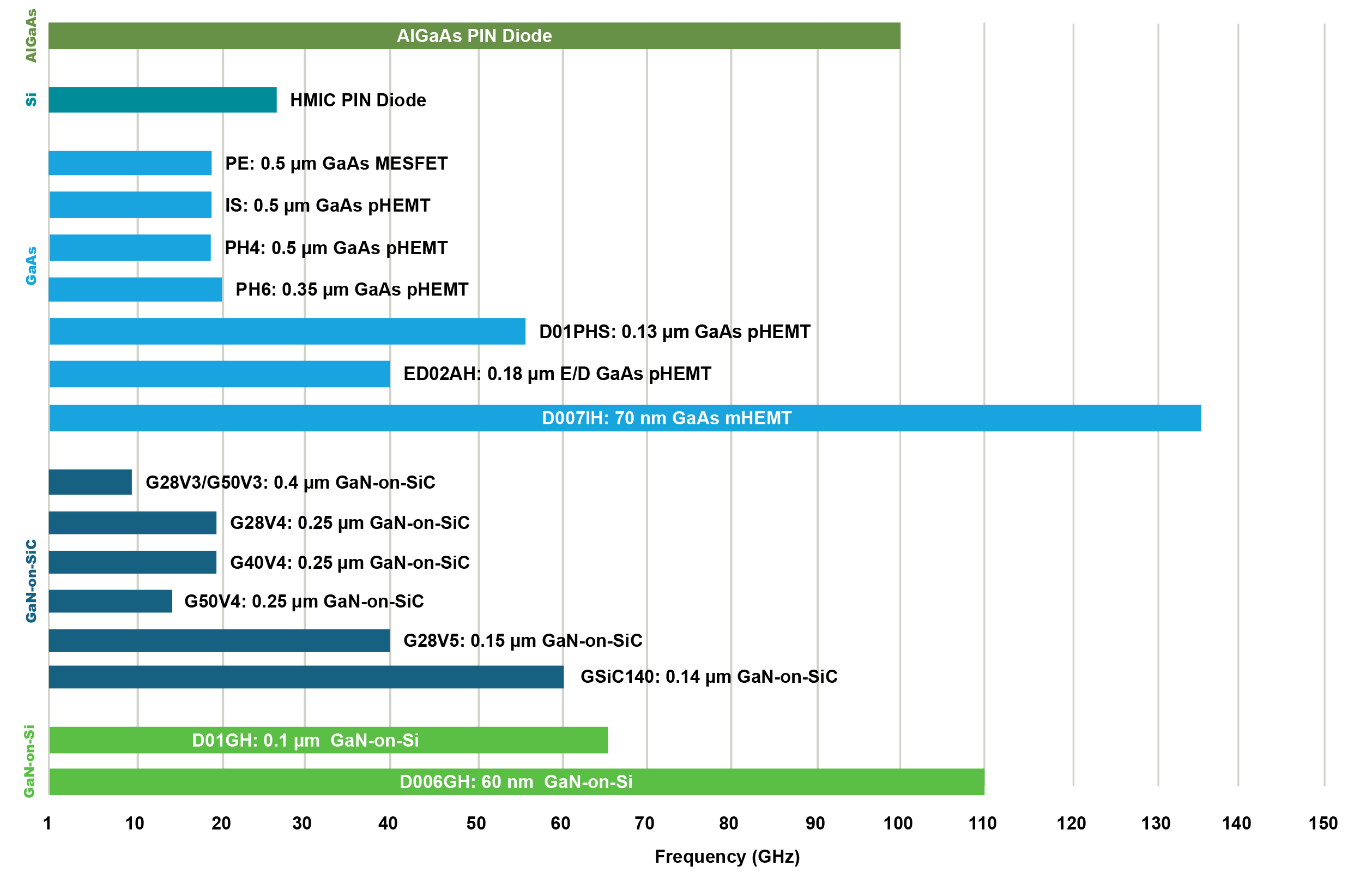
| PE | IS | PH4 | PH6 | D01PHS | ED02AH | D007IH | |
|---|---|---|---|---|---|---|---|
| Gate Length | 0.5 μm | 0.5 μm | 0.5 μm | 0.35 μm | 0.13 μm | 0.18 μm | 70 nm |
| Bias Voltage | 6 V | 6 V | 8 V | 4.5 V | 3 V | 1.25 V | |
| Breakdown Voltage | 11 V | 12 V | 14 V | 18 V | 11 V | 7.5 V | 3 V |
| RF Density | 0.65 W/mm | 0.75 W/mm | 0.9 W/mm | 0.6 W/mm | 0.4 W/mm | 0.1 W/mm | |
| Frequency Band | DC– 18 GHz | DC - 18GHz | DC - 18GHz | DC – 20 GHz | DC – 65 GHz | DC – 40 GHz | DC – 135 GHz |
| Substrate thickness | 100µm | 100µm | 100µm | 100µm | 100µm | 100µm | 100 μm 70 μm |
| Fact Sheet |
GaN-on-SiC
| G28V5 | G28V4 | G40V4 | G28V3 | G50V3 | G50V4 | GSiC140 | |
|---|---|---|---|---|---|---|---|
| Gate Length | 0.15 µm | 0.25 µm | 0.25 µm | 0.4 µm | 0.4 µm | 0.25 µm | 0.14 μm |
| Bias Voltage | 28 V | 28 V | 40 V | 28 V | 50 V | 50 V | 25 V |
| Breakdown Voltage | >84 V | >84 V | >120 V | >84 V | >150 V | >150 V | 50 V |
| RF Density | 3.75 W/mm | 4.5 W/mm | 6 W/mm | 4.5 W/mm | 8 W/mm | 8.5 W/mm | 5 W/mm |
| Frequency Band | DC - 40 GHz | DC - 18 GHz | DC - 18 GHz | DC - 8 GHz | DC - 6 GHz | DC - 14 GHz | DC – 60 GHz |
| Substrate thickness | 75µm | 100µm | 100µm | 100µm | 100µm | 100µm | 100µm |
| Fact Sheet | |||||||
| PDKs | Request | Request | Request | Request | Request | Request | Request |
| Models | Request | Request | Request | Request | Request | Request | Request |
GaN-on-Si
| D01GH | D006GH | |
|---|---|---|
| Gate Length | 0.1 µm | 0.06 µm |
| Bias Voltage | 12 V | 12 V |
| Breakdown Voltage | >36 V | >36 V |
| RF Density | 3 W/mm | 3 W/mm |
| Frequency Band | DC - 65 GHz | DC - 110 GHz |
| Substrate thickness | 100 µm | 100 µm |
| Fact Sheet | Download PDF |
Product Design Kits (PDKs) and Models
- Scalable non-linear model
- Passives created with MACOM design rules
- Full schematic-driven layout
- Real time design rule-checking
MACOM offers non-linear, scalable GaN HEMT models for MMICs, as well as full PDKs for Keysight Technologies’ Advanced Design System (ADS) and Cadence/AWR Microwave Office (MWO).
GaN Foundry Dedicated Wafers
MACOM fabricates a fully custom wafer run containing the customer’s exclusive die designs. The entire reticle is available for the customer MMIC or discrete device content. Diced, PCM-good wafers are delivered.
- Custom designs
- DRC, layout, and model support
- DC/RF on-wafer testing services optional
- Die pick and place to gel pack available
- Plastic overmold packaging services available for select lead frames
Trusted Foundry
MACOM is a DMEA Certified Trusted Foundry.
MACOM’s GaN foundry services are executed in a Defense Microelectronics Activity (DMEA) certified Category 1A trusted-foundry. We have manufacturing and statistical process controls in place to enable quick and reliable turnaround times.
Foundry Training
MACOM offers in-depth training for RF Microwave engineers who want to learn how to design in the MACOM FAB. Basic knowledge of MMIC design and experience using Microwave Office (MWO) or Advanced Design System (ADS) is required.
This training will offer RF Microwave engineers the opportunity to:
- Learn how to best utilize the PDK
- Explore HEMT and passive device models
- Understand the proper steps in designing a MMIC or HEMT
- Follow proper procedures for submitting a design